Articles
The Vital Role of RFID Technology in Semiconductor Manufacturing Process

Over the past decades, semiconductors have rapidly become a key component in all industries, from factory to fashion, from automotive to agriculture, from your desk to your kitchen, etc. These tiny semiconductors devices can transform a static appliance into a smart device from a consumer perspective. Additionally, semiconductor devices also play an important role in driving the hypergrowth of cloud computing in data centers and the fabric of networks across the globe.
It has been taken for granted that the magical process of turning silicon ingot into an electronics component is always everlastingly easy and cheap. However, after the Covid-19 pandemic spread around the world for a few months, we all experienced a global shortage of semiconductors. Suddenly, we recognized that the manufacturing linkage of micro-scale components in the semiconductor supply chain is fragile. Being aware of this risk, major industrialized countries attempt to build a more resilient semiconductor supply chain.

Building a Robust Semiconductor Supply Chain
The main reason causing the fragility of the semiconductor supply chain is offshoring technological activity. Therefore, major industrialized countries are expanding investment in local wafer fabrication and improving local manufacturing capability to create a more sophisticated supply chain, and thus fulfill the increasing demand in the semiconductor industry.

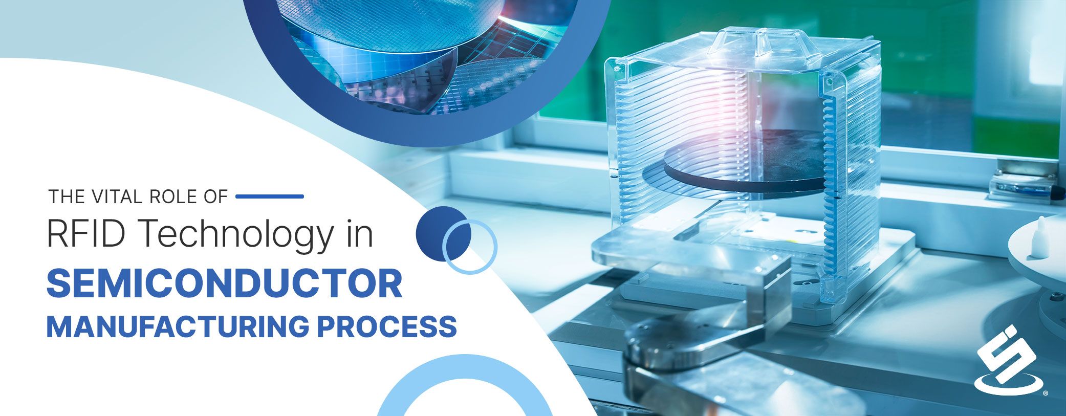
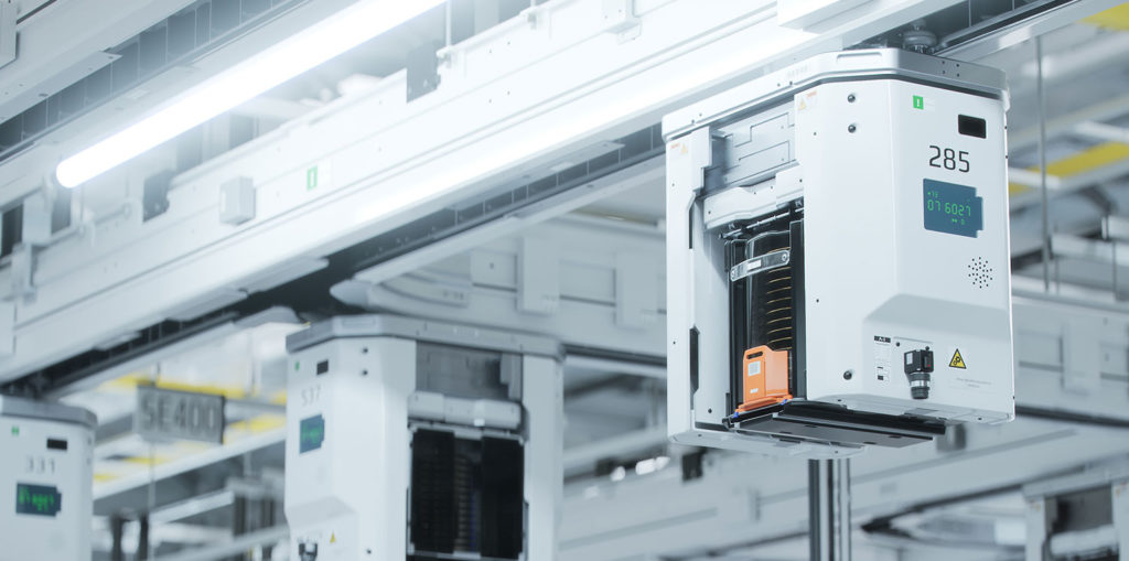
To maximize production efficiency, the new wafer factories and those under renovation are moving to a state-of-the-art semiconductor manufacturing process that relies on 300mm wafers. These wafers are huge and highly sensitive to dust and moisture. For this reason, most of the time these wafers need to be kept in FOUP (Front Opening Unified Pod), a standardized enclosure containing up to 25 wafers. The enclosure ensures a high degree of cleanliness, which is extremely important for semiconductor manufacturing, as well as unifying the material handling method throughout the process.
Wafer Tracking via RFID Technology
The 134.2kHz HDX RFID technology has been selected as the standard method for FOUP identification in the semiconductor industry due to its robustness. Not requiring a line of slight for reading, RFID technology reduces constraints in machine design and enables more compact and effective automation in semiconductor fabrication. Because RFID tags are kept inside polycarbonate material, they have the advantage of sturdiness that enable them to travel together FOUP from the start of production to the final product for up to one month.

Conclusion
To support the global expansion of the semiconductor industry, Silicon Craft Technology PLC offers SIC73F1, a 32mm LF HDX Glass Transponder, used in the FOUP application. SIC73F1 is an LF transponder with a large memory to store information according to SEMI E144-0312 standard, which is also compatible in form and function with a de-facto FOUP transponder. SIC73F1 provides more options for semiconductor equipment manufacturers through high-quality RFID technology to fulfill the rapid demand growth from new wafer fabrications around the world.


