Voltage Sensor Interface with NFC Forum Type 2 Tag IC – SIC4343
USD 3.9255
Type: RFID IC
Packing: ESD bag
PCODE: P40CVQK4P20UT4B10C2
Minimum Order Quantity: 20 pcs
Shipping: Approximately 30-45 days From Silicon Craft Technology, Bangkok, Thailand
Please note: This product is sold in minimum order quantities. Orders must meet the required MOQ to proceed. For bulk order, please direct contact us.
500 in stock
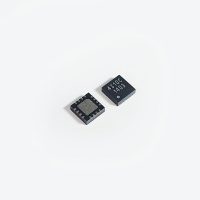
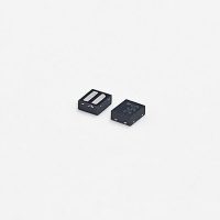
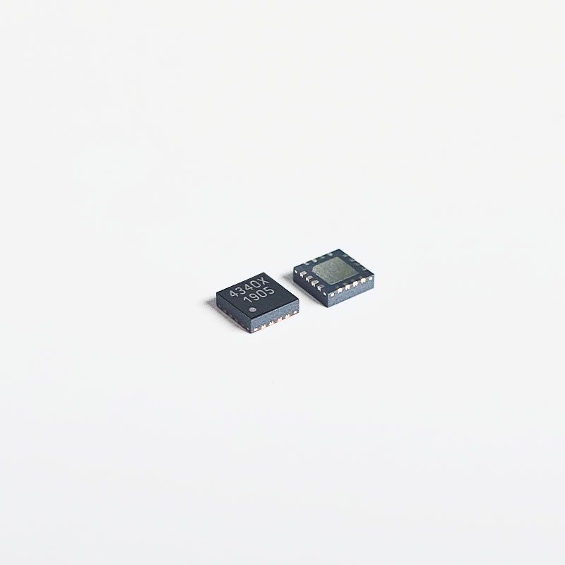
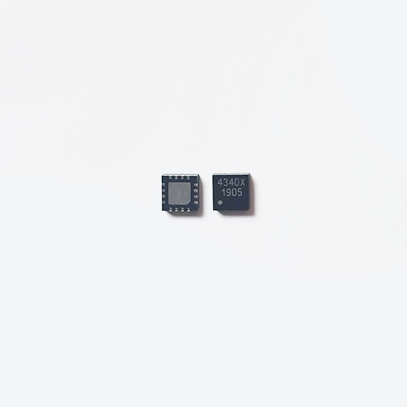
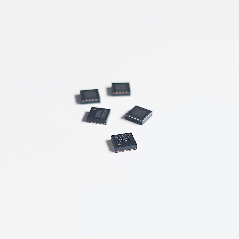
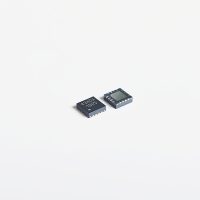
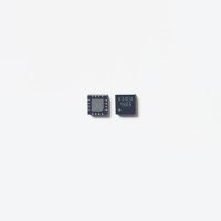
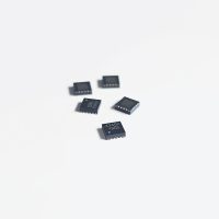
SIC4343
Voltage Sensor Interface Chip
DOWNLOAD FACTSHEET
SIC4343 is a 236-byte NFC tag IC with voltage sensor analog front-end. The SIC4343 consists of an RF Analog-Front-End circuit supporting
ISO/IEC 14443 A, a selectable 6-to-16-bit resolution sigma-delta ADC, an on-chip regulator, two 8-bit DACs, a voltage reference, a digital controller
and an EEPROM. SIC4343 is designed to perform voltage biasing and voltage measurement across sensor.
Highlight Features
- Built-In ADC
- Selectable Post Processing Average
-
Adjustable Conversion Starting Point to Avoid
-
Uplink to Ensure Power Stability
-
Configurable Built-In Voltage Buffer for High-Impedance Sensor
-
-
Adjustable Sensor Biasing Frequency for Supporting Wide Capacitance-Range Sensor
- Adjustable Sampling Point and Warm Up Clock
-
Support High Input impedance configuration
| Product Attributes | Description | |
|---|---|---|
| Specification | SIC4343 | |
| RFID Features | ||
| Working Principle |
Single-Ended Mode: Chip measures voltage |
Differential Mode: Chip measures voltage |
| Communication Interface | NFC Forum Type 2 Tag ISO/IEC 14443 A |
|
| Power Management | RF On-chip regulator 1.9 V |
|
| Number of Channels | 3 I/O 2 channels – configurable Voltage source = 2 pins ADC input = 1 pin |
3 I/O 1 channel – configurable Voltage source = 1 pin ADC differential input = 2 pins |
| Voltage Source | ||
| Bias Wave Form | DC | |
| Bias Voltage Range | 0.2 V to 1.2 V | |
| Bias Voltage Accuracy | ± 6 mV | |
| Analog Input | ||
| Input Impedance | Input buffer is enabled: > 10 MΩ Input buffer is disabled: 18 – 42 kΩ |
|
| Measured Voltage Range | Input buffer is enabled: 0.2 V to 1.2 V Input buffer is disabled: 0 V to 1.2 V |
Input buffer is enabled: -1 V to +1 V Input buffer is disabled: -1.2 V to +1.2 V |
| Measured Accuracy | ± 2.5 mV | |
| Data Conversion Rate | 10 sps | |
| Memory | ||
| User Memory | 144 bytes | |
| Erase/Write Cycles | 100,000 times | |
| Data Retention | 10 years at 70°C | |
| Others | ||
| Compatible Analysis Techniques | Open Circuit Potential (OCP), Single-ended voltage measurement |
Differential voltage measurement (resistive divider, wheatstone bridge) |
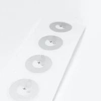
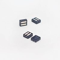
| Available Form Factors | QFN 3×3 – 16 leads, Sawn wafer with bump |
|
Applications
-
Healthcare
-
pH
-
Electrolytes (Cl-, Na+, K+, Etc.) in sweat or wound
-
Etc.
-
-
Food & Beverage Industry and Agriculture/ Environment
-
pH
-
Ions (Na+, Cl-, Mg2+, Ca2+, Cu2+, Carbonate, Etc.)
-
Etc.
-
-
Industrial Sensor
-
Strain Sensor
-
R-Divider
-
Etc.
-
- Etc.
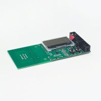
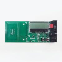
DEVELOPMENT KIT
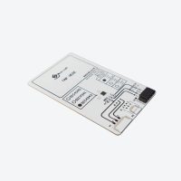
SUPPORT MATERIALS
- Demonstration software: iOS, Android application
- Reference PCB design and schematic diagram
- Reference antenna design